
[ad_1]
Hwang Cheol-seong, president of Seoul National University. Hankyung DB
On the 10th, shocking news was delivered to the Korean semiconductor industry. Micron, an American memory semiconductor company, announced that “the world’s first 176-layer NAND flash (semiconductor that stores data even when the power is off) has been manufactured and delivered to customers.”
Recently, NAND flash companies have been competing to create products with large storage capacity by vertically stacking “cells”, which are data storage spaces. Samsung Electronics and SK Hynix are focusing on 128-layer products and developing 176-layer products. Compared to one building, Samsung Electronics and SK Hynix are building 128-story buildings, but Micron is the first in the world to complete and sell a 176-story building.
In the semiconductor industry, there is a reaction that “I was vigilant and ate a shot”. In the DRAM market (semiconductor where data disappears when power is removed), Micron ranks third in the world (22.2%) after Samsung Electronics (42.1% share) and SK Hynix (30.2%) in the second quarter, but NAND In the flash market, Samsung Electronics (33.8%), Japan Kioxia (17.3%), US Western Digital (15.0%), Intel (11.5%) and SK Hynix (11 , 4%) are in 6th place (10.2%). Because.
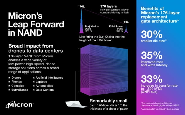
Introducing Micron’s 176-layer NAND Flash in the United States. The difference in performance between the existing product and the 176-speed product is underlined compared to the Burj Khalifa in Dubai (828m) and the Eiffel Tower in Paris (300m). Micron homepage
On the afternoon of the 13th, we heard the significance and wavelength of mass production of Micron’s 176-layer NAND flash from Hwang Chul-sung, a professor at Seoul National University (photo). Professor Hwang has served as a professor in the Department of Materials Science and Engineering at Seoul National University and the head of the Semiconductor Research Institute. As a regular member of the Academy of Science and Technology, he is a semiconductor expert who has published more than 630 scientific and technical articles on the citation index (SCI). Prior to his appointment as a professor, he worked at Samsung Electronics’ research and development center, which is rated not only for research and education, but also for industry.
Professor Hwang said: “In the field of NAND flash, Micron’s technological prowess has surpassed Samsung Electronics, or at least has become equal.” Regarding the DRAM market, he explained: “The technology gap between Samsung Electronics and Micron in the past was at the level of ‘three years’, but recently it has narrowed to ‘half a year’.” He explained, “Micron, who walked after three steps, was half a step behind.” done. Below is a summary of the questions and answers.
▶ Did Micron really succeed in mass production of 176-layer NAND?
“I don’t think it was mass produced once, but it’s a prototype.” (For reference, Micron used the expression that they have been successful in mass production.)
▶ Micron’s technology is much more than I thought.
“There is nothing special about the working principle of NAND flash (compared to other semiconductors).”
▶ Why can’t Samsung Electronics do this?
“I have to accumulate cells and drill a hole in the middle, but as the number of layers increases, it becomes more and more difficult to drill. Samsung Electronics is the only company in the world to drill holes up to 128 layers simultaneously (single stack). technology was excellent. Since it was technically impossible for Samsung Electronics to penetrate 176 simultaneously, it was a situation that had to penetrate twice (Double Stack).
▶ What is the situation at SK Hynix?
“SK Hynix originally drilled a hole twice. For example, if Samsung Electronics built a 100-story building at once, SK Hynix built 50 floors first and then 50 floors above. The 128-layer NAND is manufactured by SK Hynix. When it was first mass produced in the world, it was also made with a double hole (double stack). SK Hynix is also working hard to develop a 176 layer product. “
▶ How many times will a micron make a hole?
“I penetrated twice from the start.”
▶ What is the vibe of Samsung Electronics or SK Hynix like right now?
“Samsung Electronics in the NAND field would have been in trouble due to SK Hynix’s acquisition of Intel’s NAND division, but it was another blow. We can overcome the technical difficulties. In fact, I don’t think it’s a big difference. Samsung Electronics and SK Hynix are preparing. Probably late this year or early next year. “
▶ If so, wouldn’t I be very worried?
“The problem is, it’s important that Micron comes out first, even for a month.”
▶ It appears that Micron was not a company affected by the technology.
“I felt a sense of disparity. Actually, Micron is a conservative company. Even when it comes to producing DRAM, Samsung Electronics first uses good equipment to make good products in large quantities. Micron says,” We are First Mover’s fault. “when Samsung Electronics led the way. It was a” I’ll get “and” eat fruit “strategy.”
▶ Has the strategy changed?
“Yes. It was an operation like” We go slow even if we eat less money “, but when we see the product released first, it can be said that it has changed to” aggressive “.
▶ Why have the microns changed?
“If you release a product six months earlier, it has a great effect of worrying the market and making money. Until now, if Samsung Electronics developed and released it” first “and eats fruit from a new market, SK Hynix eats it second. level, and later Micron It was a facility like this to eat. I’m worried. “
▶ What do you think is the driving force behind the stroke and the micron exit?
“The positive effects of the acquisition of Elpida by the Japanese company DRAM are coming out now. The acquisition of Elpida by Micron has suffered a lot of financial difficulties. Now, the organization has stabilized. Especially in terms of technology because it absorbs Elpida’s research and development workforce and growing in scale. Now it works. “
(Micron, which was the fourth largest DRAM market at the time in 2013, acquired Japan’s Elpida, which is the third largest in the world. Despite the combination of third and fourth positions, it did not reach second place in the DRAM market. It was said to be a mistake, “but Professor Hwang believes the acquisition was good in terms of research and development).
▶ How should Korean semiconductor companies respond?
“In the end, it’s a manpower. Increasing research and development manpower isn’t easy. Micron’s largest acquisition of Elpida has been Elpida’s skilled R&D workforce.”
▶ Will Micron come to DRAM?
“In the past, the technology gap between Samsung Electronics and Micron was” three years. “When Samsung Electronics made the first generation of 10nm (nanometer, 1 billionth of a meter) DRAM, Micron followed long after. But now , the gap is “half a year”. Years (6 months). Now I don’t know when it will change. “
(Actually, Samsung Electronics, SK Hynix and Micron are mass production 1z products called 3rd generation 10nm products)
▶ Was it also the role of the US government?
“The memory semiconductor market is growing. The share of memory semiconductors in the total semiconductor market has increased from about 15% to about 30%. To adjust to the size of the market, the US government has also increased the support for local semiconductor companies Donald Trump’s administration said “American Great Again” shouted and supported the manufacturing industry in their country. Those things were followed at a rapid pace on their shoulders. “
▶ Will EUV change the rules of the game in the DRAM market?
“The introduction of EUV equipment into DRAM production is a strategy of” first market occupation and exhaustion “. It is true that the use of such expensive equipment is burdensome because DRAM is cheaper than CPU, etc. It is a battle on costs. If the cost increases by using expensive equipment, price competitiveness will not be satisfied. The use of expensive EUV equipment is because there is a merit that remains sufficient to offset the cost increase by increasing process efficiency ” .
▶ How do you see the DRAM market in the future?
“In the past, when we went from 40nm to 30nm and 20nm, we quickly reduced it by 10nm. But as we move to 10nm, it is becoming difficult to reduce 1nm in DRAM. I don’t know if Micron can solve DRAM. faster than Samsung Electronics or SK Hynix. Samsung Electronics has increased profits by making preemptive investments based on scale superiority so far. Using EUV over DRAM is a revolutionary change .. EUV equipment is expensive because equipment is expensive , but the money to maintain and operate the equipment is expensive. That’s a lot. As Samsung Electronics beats it, SK Hynix is following too. It will be a big game changer in the future.
Professor Hwang told reporters from the past: “The technology gap between Korean memory semiconductor companies, US-based Micron and Japan’s Kioxia is gradually narrowing,” he said. “China can catch up quickly with NAND memory, so don’t be vigilant.” I told you. Summarizing the interview, he stressed once again that “The appearance of microns after Samsung Electronics has been reduced to” 3 steps to half a step “for DRAM, and NAND is” already upside down “.”
This is why Korean semiconductor companies like Samsung Electronics and SK Hynix currently maintain a high market share in the global DRAM and NAND flash markets, which is why they are not in a situation where they will be relieved. Even in a tough business environment, Samsung Electronics invests 20 to 30 trillion won annually in the semiconductor line Pyeongtaek, Gyeonggi province, and SK Hynix spends 10 trillion won to acquire the Intel NAND division.
Reporter Hwang Jeong-soo [email protected]
Source link
