[ad_1]
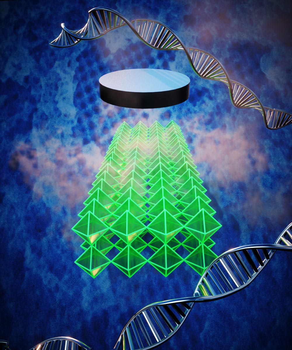
An illustration showing how highly nanostructured 3-D superconducting materials can be created on the basis of DNA self-assembly. Credit: Brookhaven National Laboratory
Complex 3D nanoscale architectures based on DNA self-assembly can conduct electricity without resistance and can provide a platform for fabrication quantum computing and detection devices
Three-dimensional (3-D) nanostructured materials – those with complex shapes on a dimensional scale of billionths of a meter – that can conduct electricity without resistance could be used in a range of quantum devices. For example, such 3-D superconducting nanostructures could find application in signal amplifiers to improve speed and precision of quantum computers and ultra-sensitive magnetic field sensors for medical imaging and geological mapping of the subsoil. However, traditional fabrication tools such as lithography have been limited to 1-D and 2-D nanostructures such as superconducting wires and thin films.
Now, scientists from the US Department of Energy’s (DOE) Brookhaven National Laboratory, Columbia Universityand Bar-Ilan University in Israel have developed a platform to build 3-D superconducting nano-architectures with prescribed organization. As reported in the November 10, 2020 issue of Nature Communications, this platform is based on the self-assembly of DNA into desired 3-D forms at the nanoscale. In DNA self-assembly, a single long strand of DNA is folded from shorter strands of complementary “staple” into specific positions – similar to origami, the Japanese art of folding paper.
“Thanks to its structural programmability, DNA can provide an assembly platform for building engineered nanostructures,” said co-correspondent author Oleg Gang, leader of the Soft and Bio Nanomaterials Group at Brookhaven Lab’s Center for Functional Nanomaterials ( CFN) and professor of engineering chemistry and applied physics and materials science at Columbia Engineering. “However, the fragility of DNA makes it seem unsuitable for fabrication of functional devices and nano-fabrication that requires inorganic materials. In this study, we have shown how DNA can serve as a scaffold for building three-dimensional nanoscale architectures that can be completely “converted” into inorganic materials such as superconductors.
To make the scaffold, scientists from Brookhaven and Columbia Engineering first designed octahedral-shaped DNA origami “frames”. Aaron Michelson, Gang’s graduate student, applied a programmable DNA strategy so that these frames assemble into desired lattices. Then, he used a chemical technique to coat the DNA lattices with silicon dioxide (silica), solidifying the originally soft constructions, which required a liquid environment to preserve their structure. The team adapted the fabrication process so that the structures were faithful to their design, as confirmed by imaging at the CFN Electron Microscopy Facility and small-angle X-ray scattering at the scattering beam line of complex materials from the Brookhaven National II synchrotron light source (NSLS-II). These experiments showed that structural integrity was preserved after coating the DNA lattices.
“In its original form, DNA is completely unusable for processing with conventional nanotechnology methods,” said Gang. “But once DNA is coated with silica, we have a mechanically robust 3-D architecture on which we can deposit inorganic materials using these methods. This is analogous to traditional nanofabrication, in which valuable materials are deposited on flat substrates, typically silicon, to add functionality “.
The team shipped the silica-coated DNA lattices from the CFN to the Bar-Ilan Institute of Superconductivity, led by Yosi Yeshurun. Gang and Yeshurun met a couple of years ago when Gang gave a seminar on his research on DNA assembly. Yeshurun - who for the past decade has been studying the properties of superconductivity at the nanoscale – thought that Gang’s DNA-based approach could provide a solution to a problem he was trying to solve: how can we fabricate superconducting structures at the nanoscale in three dimensions?
“Previously, making 3-D nanosuperconductors required a very elaborate and difficult process using conventional fabrication techniques,” said Yeshurun, corresponding co-author. “Here, we have found a relatively simple way using Oleg’s DNA structures.”
At the Institute of Superconductivity, Yeshurun graduate student Lior Shani evaporated a low-temperature superconductor (niobium) onto a silicon chip containing a small sample of the lattices. The evaporation rate and temperature of the silicon substrate had to be carefully controlled so that the niobium coated the sample but did not penetrate completely. If this happens, a short circuit may occur between the electrodes used for electronic transport measurements.
“We cut a special channel in the substrate to ensure that the current only flows through the sample itself,” explained Yeshurun.
The measurements revealed a 3-D matrix of Josephson junctions, or thin non-superconducting barriers through which superconducting current tunnels. Josephson junction arrays are critical for exploiting quantum phenomena in practical technologies, such as superconducting quantum interference devices for magnetic field detection. In 3-D, multiple junctions can be grouped into a small volume, increasing the power of the device.
“DNA origami has produced beautiful and ornate three-dimensional nanoscale structures for nearly 15 years, but DNA itself is not necessarily a useful functional material,” said Evan Runnerstrom, program manager for materials design at the US Army. Combat Capabilities Development Command Army Research Laboratory of the US Army Research Office, which partly funded the work. “What Prof. Gang showed here is that it is possible to exploit DNA origami as a template to create useful 3-D nanostructures of functional materials, such as superconducting niobium. This ability to arbitrarily design and fabricate complex 3-D structured functional materials from the bottom up will accelerate the army’s modernization efforts in areas such as sensing, optics and quantum computing. “
“We have demonstrated a path for how complex DNA organizations can be used to create highly nanostructured 3-D superconducting materials,” said Gang. “This material conversion path gives us the ability to build a variety of systems with interesting properties – not only superconductivity but also other electronic, mechanical, optical and catalytic properties. We can imagine it as a “molecular lithography”, in which the power of DNA programmability is transferred to the inorganic 3-D nanofabrication. “
Reference: 10 November 2020, Nature Communications.
DOI: 10.1038 / s41467-020-19439-9
This research was supported by the US Department of Defense, Army Research Office; DOE Office of Science; Israeli Ministry of Science and Technology; and Israel Science Foundation. Both CFN and NSLS-II are facilities for users of the DOE Office of Science. Some imaging studies were performed at the City University of New York Advanced Science Research Center’s Imaging Facility.
[ad_2]
Source link
