[ad_1]
(Nanowerk News) The performance of large-area flexible organic photodiodes has advanced to the point that they can now offer advantages over conventional silicon photodiode technology, particularly for applications such as biomedical imaging and biometric monitoring that require low-light detection over large areas.
The low-noise, flexible organic devices elaborated in solution offer the ability to use arbitrary shaped large area photodiodes to replace complex arrays that would be required with conventional silicon photodiodes, which can be expensive to scale for large area applications. Organic devices provide performance comparable to rigid silicon photodiodes in the visible light spectrum ?? except in the response time.
What we have obtained is the first demonstration that these devices, produced from a solution at low temperatures, can detect even a few hundred thousand photons of visible light every second, similar to the magnitude of the light reaching our eye from a single star in a dark sky, ?? said Canek Fuentes-Hernandez, principal investigator at the School of Electrical and Computer Engineering at the Georgia Institute of Technology. • The ability to coat these materials on large area substrates with arbitrary shapes means that flexible organic photodiodes now offer some clear advantages over state-of-the-art silicon photodiodes in applications requiring response times of the order of tens of microseconds. ?
The development and performance of large-scale low-noise organic photodiodes are described in the journal Science (“Large Area Low Noise Flexible Organic Photodiodes for Detection of Weak Visible Light”).

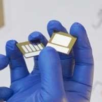
Organic electronic devices rely on materials manufactured from carbon-based molecules or polymers instead of conventional inorganic semiconductors such as silicon. The devices can be made using simple solutions and inkjet printing techniques instead of the costly and complex processes involved in conventional electronics manufacturing. The technology is now widely used in displays, solar cells and other devices.
Organic photodiodes use polyethyleneimine, an amine-containing polymer surface modifier found to produce air-stable, low-work function electrodes in photovoltaic devices developed in the laboratory of Bernard Kippelen, Joseph M. Pettit Professor at Georgia Tech. The use of polyethyleneimine has also been shown to produce photovoltaic devices with low levels of dark current ?? the electric current flowing through a device even in the dark. This meant that the materials could be useful in photodetectors for capturing faint visible light signals.
?? Over the years, dark current levels have been reduced so much that measurement equipment had to be redesigned to detect an electronic noise corresponding to a fluctuation of one electron in one millionth of a second Fuentes-Hernandez, the first author of the paper. he said. ?? This work reflects the sustained team efforts made in the Kippelen group for more than six years and includes part of the PhD. work of recent graduates Talha Kahn and Wen-Fang Chou. These collective efforts have yielded the scientific knowledge necessary to demonstrate organic photodiodes with this level of performance.
One application for the new devices is in pulse oximeters now placed on fingers to measure heart rate and blood oxygen levels. Organic photodiodes can allow multiple devices to be placed on the body and operate with 10 times less light than conventional devices. This could allow wearable health monitors to produce improved physiological information and continuous monitoring without frequent battery changes. Other potential applications include human-computer interfaces such as contactless gesture recognition and controls.
Is the detection of ionizing radiation by scintillation a future application? a flash of light emitted by a phosphor when struck by a high-energy particle. Lowering the detectable light level would improve the sensitivity of the device, allowing it to detect lower levels of radiation. Detection of radiation emitted by cargo vehicles or containers requires a large detection area, which would be easier to obtain from organic photodiodes than from silicon photodiode arrays.
Organic photodiodes could have similar advantages in X-ray equipment, where doctors want to use the lowest possible level of radiation to minimize the dose delivered to the patient. Again, sensitivity, large area, and flexible form factor should give organic photodiodes an advantage over silicon-based arrays.
?? We are working to improve the response time of the photodetector because producing fast photodetectors would allow many other important applications, ?? Fuentes-Hernandez said. There is a real need to develop more scalable photodetector technologies and one of the motivations for this work is to advance organic technology that we know is convenient for scaling.
Organic photodiodes can exhibit electronic noise current values of the order of tens of femtoampere and noise-equivalent power values of a couple of hundred femtowatts. The key performance factors of organic photodiodes compare well to silicon except in the response time area, where researchers are working on a hundredfold improvement to enable future applications.
?? Since we use materials processed from inks using printing techniques, they are not as ordered as crystalline materials, ?? Kippelen said. Consequently, the mobility of carriers and the speed of carriers that can move through these materials are lower, so it is not possible to obtain the same fast signals that are obtained with silicon. But a response time of picoseconds or nanoseconds is not required for many applications.
For Kippelen, the photodiode work shows the results of a 25-year effort to improve the performance of organic electronic materials. That job, which is part of Georgia Tech ?? s Center for Organic Photonics and Electronics, involved extensive device modeling to understand basic science and research to continuously increase material performance.
?? Organic thin films absorb light more efficiently than silicon, so the overall thickness needed to absorb that light is very small, ?? Kippelen said. • Even if their area is increased, the overall volume of the detector remains small with organic substances. If you increase the area of a silicon detector, you have a larger volume of materials which will generate a lot of electronic noise at room temperature.
The photodiodes made in the Kippelen laboratory use an active layer only 500 nanometers thick. An ounce of material, about the size of a fingertip, could coat the surface of an office desk.
Kippelen hopes the Science the paper will help open new doors for organic semiconductors.
?? Advances like this will allow us to change the common belief that switching to organic materials that can lead to scalable devices would mean sacrificing performance, ?? He said. ?? We cannot anticipate all the new applications that may be enabled by this advance.
Source link
