[ad_1]

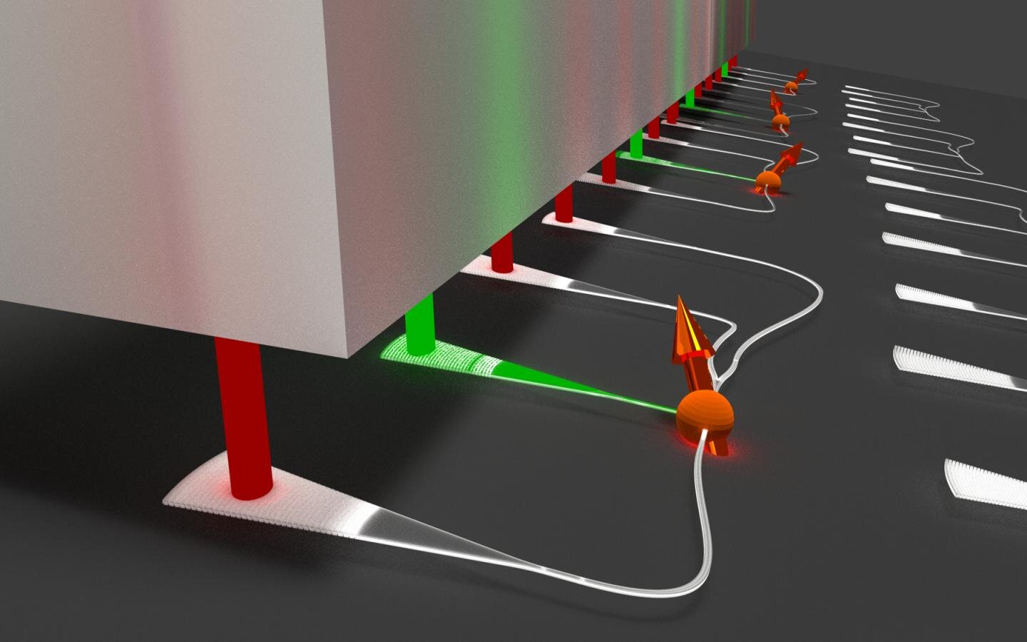
Nanophotonic integration for the simultaneous control of a large number of quantum mechanical turns in nanodiamonds. Credit: P. Schrinner / AG Schuck
Using modern nanotechnologies, it is now possible to produce structures that have a characteristic size of a few nanometers. This world of the finest particles, also known as quantum systems, makes possible a wide range of technological applications, in fields that include magnetic field sensing, information processing, secure communication or ultra-precise timekeeping. The production of these microscopically small structures has progressed so far that they reach dimensions below the wavelength of light. In this way, it is possible to break down the boundaries previously existing in optics and use the quantum properties of light. In other words, nanophotonics represents a new approach to quantum technologies.
As individual photons move in the quantum regime, scientists describe the relevant light sources as quantum emitters that can be incorporated into nanodiamonds, among others. These special diamonds are characterized by their very small particle size, which can range from a few to several hundred nanometers. Researchers from the University of Münster have now succeeded for the first time in fully integrating nanodiamonds into nanophotonic circuits and at the same time optically addressing many of these nanodiamonds. In the process, the green laser light is directed at the color centers in the nanodiamonds and the individual red photons generated are emitted in a network of optical components at the nanoscale. As a result, researchers can now control these quantum systems in a fully integrated state. The results were published in the journal Nano Letters.
Background and methodology
Previously, bulky microscopes had to be installed to control such quantum systems. With manufacturing technologies similar to those for manufacturing computer processor chips, light can be directed in a similar way using waveguides (nanofibers) on a silicon chip. These optical waveguides, measuring less than a micrometer, were produced with electron beam lithography and reactive ion etching equipment at the Münster Nanofabrication Facility (MNF).
“Here, the size of a typical experimental setup has been reduced to a few hundred square micrometers,” explains Professor Carsten Schuck of the Physics Institute of the University of Münster, who led the study in collaboration with assistant professor Doris Reiter of the Institute of Solid State Theory. “This downsizing not only means we can save space for future applications involving large numbers of quantum systems,” he adds, “but it also allows us, for the first time, to control several quantum systems of this type simultaneously.”
In preliminary work prior to the current study, the Münster scientists developed suitable interfaces between nanodiamonds and nanophotonic circuits. These interfaces have been used in new experiments, implementing the coupling of quantum emitters with waveguides in a particularly effective way. In their experiments, physicists used the so-called Purcell effect, which causes the nanodiamond to emit individual photons with a higher probability in the waveguide, rather than in a random direction.
The researchers also managed to run two magnetic field sensors, based on the integrated nanodiamonds, in parallel on a chip. Previously, this had only been possible individually or later. To make this possible, the researchers exposed the embedded nanodiamonds to microwaves, thus inducing changes in the quantum state (spin) of the color centers. The spin orientation affects the brightness of the nanodiamonds, which was subsequently read using on-chip optical access. The frequency of the microwave field and therefore the observable brightness variations depend on the magnetic field at the position of the nanodiamond. “The high sensitivity to a local magnetic field makes it possible to build sensors with which individual bacteria and even single atoms can be detected,” explains Philip Schrinner, lead author of the study.
First of all, the researchers calculated the nanophotonic interface designs using elaborate 3-D simulations, thus determining the optimal geometries. They then assembled and fabricated these components in a nanophotonic circuit. After the nanodiamonds were integrated and characterized using adapted technology, the team of physicists performed quantum mechanical measurements using a custom set-up for the purpose.
“Working with diamond-based quantum systems in nanophotonic circuits allows for a new kind of accessibility, as we are no longer limited by microscope configurations,” says Doris Reiter. “Using the method we have presented, it will be possible in the future to monitor and read a large number of these quantum systems simultaneously on one chip,” he adds. The researchers’ work creates the conditions to allow further studies in the field of quantum optics, studies in which nanophotonics can be used to modify the photo-physical properties of diamond emitters. In addition to this, there are new application possibilities in the field of quantum technologies, which will benefit from the properties of integrated nanodiamonds, for example in the field of quantum sensing or quantum information processing.
The next steps will include the implementation of quantum sensors in the field of magnetometry, used for example in the analysis of materials for semiconductor components or brain scans. “To this end,” says Carsten Schuck, “we want to integrate a large number of sensors on a chip that can all be read at the same time, and thus not only record the magnetic field at one point, but also visualize the gradients of the magnetic field in space. . ”
Physicists couple key components of quantum technologies
Philip PJ Schrinner et al, Integration of Diamond-Based Quantum Emitters with Nanophotonic Circuits, Nano Letters (2020). DOI: 10.1021 / acs.nanolett.0c03262
Provided by the University of Münster
Quote: Fully integrated nanodiamond control (2020, November 23) retrieved November 23, 2020 from https://phys.org/news/2020-11-fully-nanodiamonds.html
This document is subject to copyright. Aside from any conduct that is correct for private study or research purposes, no part may be reproduced without written permission. The content is provided for informational purposes only.
[ad_2]
Source link
