
[ad_1]
In the field of hardware we are currently witnessing a real revolution and evolution. Speaking specifically of chip lithography, 5nm manufacturing is already in full swing, but the news doesn’t stop there.
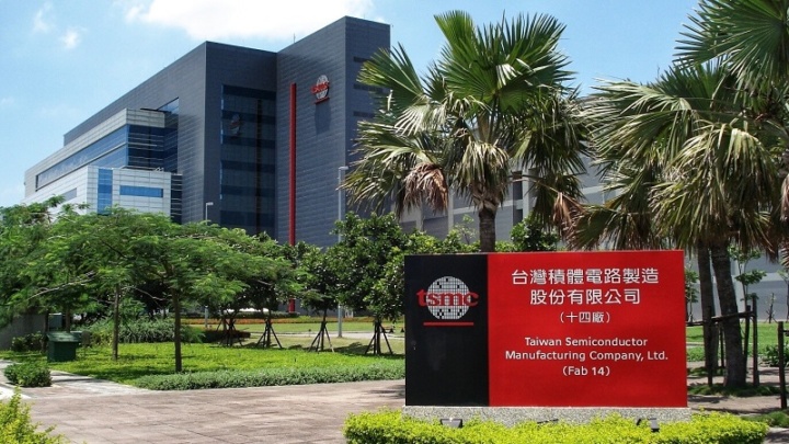
Semiconductor giant TSMC has already finished its 3nm plant and mass production is expected to start as early as 2022.
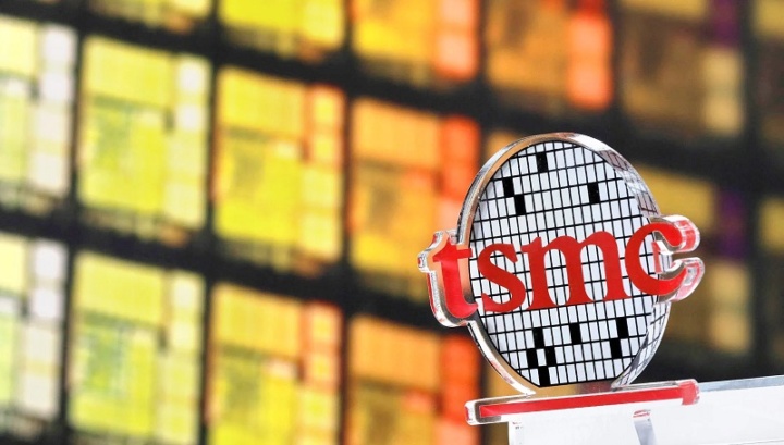
TSMC (Taiwan Semiconductor Manufacturing Company) is the largest independent semiconductor manufacturer in the world. The future of many devices is in your hands, such as processors and graphics cards.
But the company is already much more advanced when it comes to lithography of its chips. This is because some manufacturers have not stopped producing at 10nm, such as Intel.
It was recently revealed that the production of Taiwanese 5nm and 7nm chips is already in full swing by mid-2021. In addition, most of the orders for 5nm lithography have been placed by Apple, ahead of production. of the new iPhone 12. But TSMC is even more ambitious than that.
TSMC: 3nm factory is ready and mass production starts in 2022
The Taiwanese manufacturer already has its new plant ready for the production of chips in 3nm lithography. This plant is located in the Southern Taiwan Science Park, and mass production of these components is projected to begin in the second half of 2022.
The new facilities began construction at the end of October 2019 and the estimated cost for the works is $ 19.5 billion (~ € 16.3 billion).
During the presentation ceremony, Mark Liu, president of TSMC, revealed that the plant will have a production capacity of about 55 thousand pods per month in the 3nm process. Usually the manufacturer's capacity is 100 thousand pods monthly.
In the coming months, the equipment will be brought to the facility and the plant will be ready for use within a year and a half. As soon as it is operational, the new plant will have around 20,000 employees.
3nm chips promise 15% higher performance
TSMC's 3nm manufacturing process will use FinFET transistor structures and is designed for high performance mobile devices. This technology promises to deliver 15% higher performance, a 30% reduction in power consumption and a 70% increase in logical density.
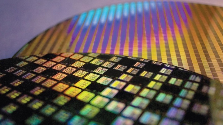
In turn, the TechPowerUp website indicates that these chips use extreme ultraviolet lithography (EUVL) up to 20 layers. This information is in line with the Twinscan NXE extreme ultraviolet (EUV) scanner orders that the manufacturer made to ASML.
Read also:
[ad_2]
Source link
