[ad_1]
(Nanowerk News) Deformation engineering usually refers to a type of material processing technology, which aims to adjust the properties of materials or optimize the performance of related devices by either intrinsic or external deformation.
In recent years, with the development of 2D materials, deformation engineering research of 2D materials (transition metal dichalcogenides (TMDC), graphene, etc.) has attracted significant attention. Compared to traditional bulk material deformation engineering, the atomic thickness of 2D materials makes them more suitable to serve as a platform for deformation engineering research and creates a bridge between deformation engineering and nanophotonics. Hence, they are worthy of attention from many points of view, from fundamental physics to practical applications.
In a new article published in Light: science and applications (“2D Semiconductor and Graphene Deformation Engineering: From Strain Fields to Band Structure Tuning and Photonic Applications”), a team of scientists, led by Dr Dangyuan Lei from the Department of Materials Science and Engineering, City University of Hong Kong, China, and colleagues wrote a review article to comprehensively summarize recent developments in this thriving field.
In this review article, the traditional macroscopic strain field theory is first introduced. Then, the band structure modifications of deformed 2D semiconductors (TMDCs) and stretched graphene are discussed, while the optical responses observed under different types of strain fields are reviewed. Next, this paper summarizes deformation engineering techniques that can apply different types of deformations to specific 2D materials.
At the end of this article, the different applications in optical devices, optoelectronics and other applications of photonics are presented and the existing problems in this field and their future development are outlined respectively.
Traditional deformation engineering primarily focuses on silicon, germanium and other 3D bulk materials, which usually lack high fracture strength due to their inherent 3D properties. Therefore, increasing 2D materials with atomic thickness (such as graphene, TMDC) have entered the field of view. Their strain engineering has been extensively studied in both the scientific community and industrial society.
Compared to traditional 3D materials, the 2D characteristics of 2D materials give them some completely different and new characteristics, making their deformation engineering more attractive.
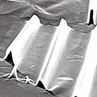
These scientists summarize those unique properties of 2D materials: “Based on the following three points, we believe 2D materials are a perfect platform for deformation engineering: (1) 2D materials have better mechanical properties (deformation ability), meaning they can withstand greater deformation before fracture than bulk materials; (2) 2D materials have better optical properties due to their strong exciton effects, which benefit their further applications in photonic devices; and (3) i 2D materials have more variable deformation patterns. Their atomic thickness properties allow them to achieve out-of-plane deformation, which is nearly impossible in 3D bulk materials, allowing 2D materials to possess multiple deformation patterns, such as uniaxial and biaxial deformation. in the plane, wrinkles, folds and localized non-uniform deformation. ”
“Because the types of deformation applied are varied, the changes in electrical and optical properties are different. In general, we can observe the red shifted (blue shift) PL spectra from tensile (compression) deformed 2D TMDCs. way, we can observe the displacement and division of the Raman spectra from the stretched graphene. Furthermore, many new optical responses, such as the ‘funnel’ effect, the emission of a single photon and the generation of tunable second harmonic, emerge under a special distribution of tension. they added.
“There are various technologies to apply strains to 2D materials. Based on the type of induced strain, we have usually classified them into three categories, namely, uniaxial deformation technologies, biaxial deformation technologies and local deformation technologies. . We should pay more attention to local deformation technologies. They actually provide a new way to control photons in an ultra-small area. In conclusion, the flexibility and optical properties of 2D materials (compared to their bulky counterparts) open the door. leads to the development of potentially important new photonic technologies, “predict the scientists.
Source link
